
The most common place silicon wafers are used is in integrated circuits, which is what powers our electronic devices. This alone should let you know how important it is that these fragile pieces of technology are finely crafted. Fortunately, silicon is the second most common element on the planet, coming in second to oxygen. Even if we were to run out of silicon here on Earth, it’s also the seventh most common element in the universe, suggesting it will never become rare or unattainable.
That’s good news for silicon wafer suppliers and for those of us who rely heavily on our electronic devices. If silicon is so common, why don’t we see it everywhere we go? In truth, the vast majority of us do see and touch silicon more often than we realize, especially when we go to the beach. Most of the silicon used to create wafers is taken from the sands of Australian beaches because this sand is especially clean. The cleaner the sand, the higher quality the silicon wafer.
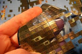
Over the years, silicon wafers have grown larger in diameter. In the early 60s, a typical silicon wafer had a diameter of just one inch, but today’s wafers are as large as 12 inches. In the future, tech experts expect these semiconducting wafers to grow to 18 inches in diameter, which will improve their usefulness.
While the surface of all wafers are generally the same diameter, the thickness of each wafer will vary. Wafer thickness will depend on its use and on the materials the wafer is intended to support. The wafer must be thick enough to protect against cracking, so it can be used for a long period of time. If the wafer cracks under its own weight, it will no longer be useful.
These facts can help you decide on the best silicon wafers to fulfill your needs. Choosing the right wafer will help you produce a quality product that will last for a longer period. It can also help ensure your device will handle the uses for which it’s intended.